- 您现在的位置:买卖IC网 > Sheet目录312 > AT25640T1-10TI-2.7 (Atmel)IC EEPROM 64KBIT 3MHZ 14TSSOP
�� �
�
�AT25080/160/320/640�
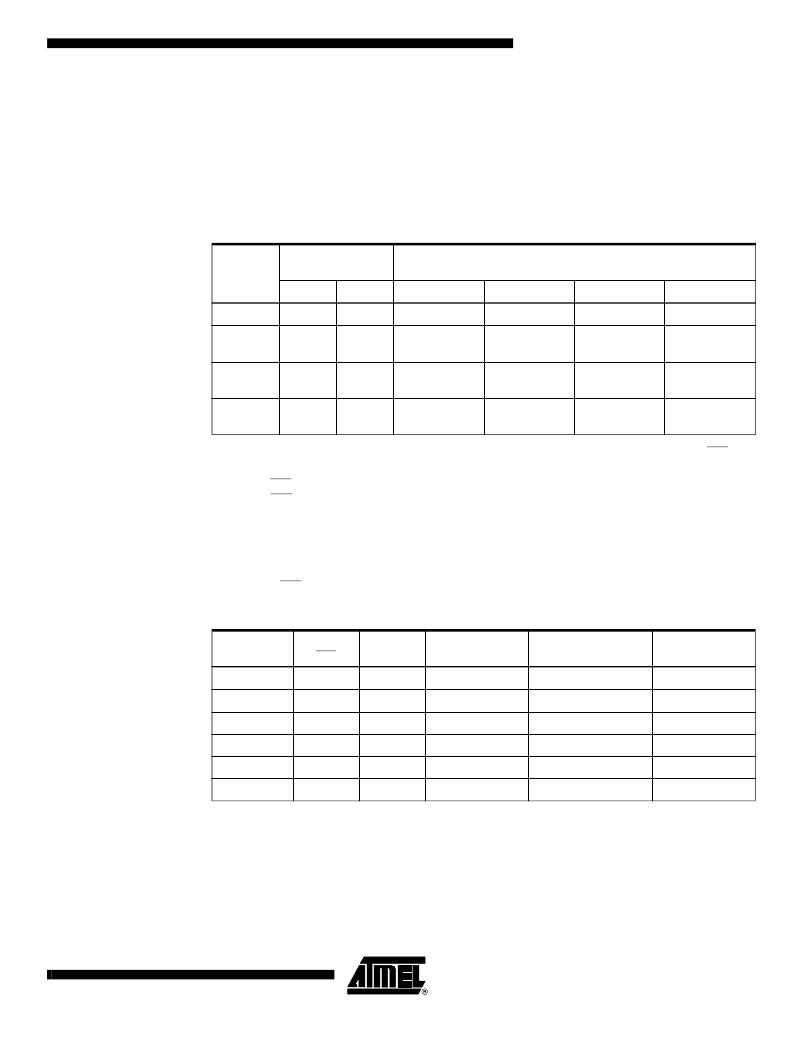
�WRITE� STATUS� REGISTER� (WRSR):� The� WRSR� instruction� allows� the� user� to� select� one� of�
�four� levels� of� protection.� The� AT25080/160/320/640� is� divided� into� four� array� segments.� One�
�quarter� (1/4),� one� half� (1/2),� or� all� of� the� memory� segments� can� be� protected.� Any� of� the� data�
�within� any� selected� segment� will� therefore� be� READ� only.� The� block� write� protection� levels� and�
�corresponding� status� register� control� bits� are� shown� in� Table� 4.�
�The� three� bits,� BP0,� BP1,� and� WPEN� are� nonvolatile� cells� that� have� the� same� properties� and�
�functions� as� the� regular� memory� cells� (e.g.� WREN,� t� WC� ,� RDSR).�
�Table� 4.� Block� Write� Protect� Bits�
�Status�
�Register� Bits�
�Array� Addresses� Protected�
�Level�
�0�
�1(1/4)�
�2(1/2)�
�3(All)�
�BP1�
�0�
�0�
�1�
�1�
�BP0�
�0�
�1�
�0�
�1�
�AT25080�
�None�
�0300�
�-03FF�
�0200�
�-03FF�
�0000�
�-03FF�
�AT25160�
�None�
�0600�
�-07FF�
�0400�
�-07FF�
�0000�
�-07FF�
�AT25320�
�None�
�0C00�
�-0FFF�
�0800�
�-0FFF�
�0000�
�-0FFF�
�AT25640�
�None�
�1800�
�-1FFF�
�1000�
�-1FFF�
�0000�
�-1FFF�
�The� WRSR� instruction� also� allows� the� user� to� enable� or� disable� the� write� protect� (WP)� pin�
�through� the� use� of� the� Write� Protect� Enable� (WPEN)� bit.� Hardware� write� protection� is� enabled�
�when� the� WP� pin� is� low� and� the� WPEN� bit� is� “1”.� Hardware� write� protection� is� disabled� when�
�either� the� WP� pin� is� high� or� the� WPEN� bit� is� “0”.� When� the� device� is� hardware� write� protected,�
�writes� to� the� Status� Register,� including� the� Block� Protect� bits� and� the� WPEN� bit,� and� the� block-�
�protected� sections� in� the� memory� array� are� disabled.� Writes� are� only� allowed� to� sections� of� the�
�memory� which� are� not� block-protected.�
�NOTE:� When� the� WPEN� bit� is� hardware� write� protected,� it� cannot� be� changed� back� to� “0”,� as�
�long� as� the� WP� pin� is� held� low.�
�Table� 5.� WPEN� Operation�
�Protected�
�Unprotected�
�Status�
�WPEN�
�0�
�0�
�1�
�1�
�X�
�X�
�WP�
�X�
�X�
�Low�
�Low�
�High�
�High�
�WEN�
�0�
�1�
�0�
�1�
�0�
�1�
�Blocks�
�Protected�
�Protected�
�Protected�
�Protected�
�Protected�
�Protected�
�Blocks�
�Protected�
�Writable�
�Protected�
�Writable�
�Protected�
�Writable�
�Register�
�Protected�
�Writable�
�Protected�
�Protected�
�Protected�
�Writable�
�9�
�0675M–SEEPR–9/03�
�发布紧急采购,3分钟左右您将得到回复。
相关PDF资料
AT25DF321-SU
IC FLASH 32MBIT 70MHZ 8SOIC
AT25F1024AN-10SU-2.7
IC FLASH 1MBIT 33MHZ 8SOIC
AT25F2048N-10SU-2.7
IC FLASH 2MBIT 33MHZ 8SOIC
AT25F4096W-10SU-2.7
IC FLASH 4MBIT 33MHZ 8SOIC
AT25HP512W2-10SI-2.7 SL383
IC EEPROM 512KBIT 10MHZ 16SOIC
AT26DF081A-SSU
IC FLASH 8MBIT 70MHZ 8SOIC
AT26DF161-SU
IC FLASH 16MBIT 66MHZ 8SOIC
AT26DF161A-MU
IC FLASH 16MBIT 70MHZ 8QFN
相关代理商/技术参数
AT25640T2-10TC
制造商:ATMEL 制造商全称:ATMEL Corporation 功能描述:SPI Serial E2PROMs
AT25640T2-10TC-1.8
制造商:ATMEL 制造商全称:ATMEL Corporation 功能描述:SPI Serial EEPROMs
AT25640T2-10TC-2.7
制造商:ATMEL 制造商全称:ATMEL Corporation 功能描述:SPI Serial EEPROMs
AT25640T2-10TI
制造商:ATMEL 制造商全称:ATMEL Corporation 功能描述:SPI Serial EEPROMs
AT25640T2-10TI-1.8
功能描述:IC EEPROM 64KBIT 3MHZ 20TSSOP RoHS:否 类别:集成电路 (IC) >> 存储器 系列:- 标准包装:32 系列:- 格式 - 存储器:闪存 存储器类型:FLASH 存储容量:1M (128K x 8) 速度:120ns 接口:并联 电源电压:2.7 V ~ 3.6 V 工作温度:0°C ~ 70°C 封装/外壳:32-LCC(J 形引线) 供应商设备封装:32-PLCC 包装:管件 其它名称:AT49BV00112JC
AT25640T2-10TI-2.7
功能描述:IC EEPROM 64KBIT 3MHZ 20TSSOP RoHS:否 类别:集成电路 (IC) >> 存储器 系列:- 标准包装:32 系列:- 格式 - 存储器:闪存 存储器类型:FLASH 存储容量:1M (128K x 8) 速度:120ns 接口:并联 电源电压:2.7 V ~ 3.6 V 工作温度:0°C ~ 70°C 封装/外壳:32-LCC(J 形引线) 供应商设备封装:32-PLCC 包装:管件 其它名称:AT49BV00112JC
AT25640W-10SC-1.8
功能描述:IC EEPROM 64KBIT 3MHZ 8SOIC RoHS:否 类别:集成电路 (IC) >> 存储器 系列:- 标准包装:378 系列:- 格式 - 存储器:闪存 存储器类型:FLASH 存储容量:8M(1M x 8,512K x 16) 速度:110ns 接口:并联 电源电压:2.7 V ~ 3.6 V 工作温度:-40°C ~ 85°C 封装/外壳:48-CBGA 供应商设备封装:48-CBGA(7x7) 包装:托盘
AT25640W-10SI-2.7
功能描述:IC EEPROM 64KBIT 3MHZ 8SOIC 制造商:microchip technology 系列:- 包装:管件 零件状态:停產 存储器类型:非易失 存储器格式:EEPROM 技术:EEPROM 存储容量:64Kb (8K x 8) 时钟频率:3MHz 写周期时间 - 字,页:5ms 存储器接口:SPI 电压 - 电源:2.7 V ~ 5.5 V 工作温度:-40°C ~ 85°C(TA) 安装类型:表面贴装 封装/外壳:8-SOIC(0.154",3.90mm 宽) 供应商器件封装:8-SOIC 基本零件编号:AT25640 标准包装:94